DDR1
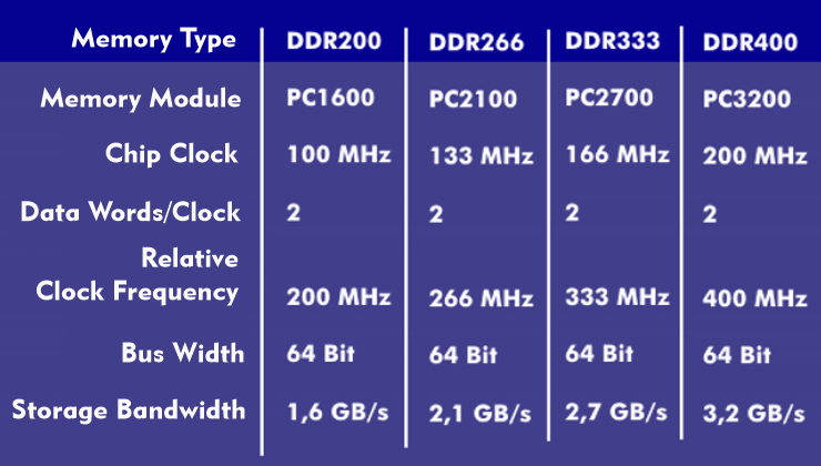
DDR technology is standardized by the Joint Electron Device Engineering Council( JEDEC). DDR1 operates at clock frequencies of 100 MHz, 133 MHz, 166 MHz and 200 MHz. The relative clock rate is doubled by Double Date Rate (DDR).
DDR1 memory chips have a supply voltage of 2.5 V and 64-bit bus width. Columm Access Strobe ( CAS) latency is 2.5, access times range from 3.5 ns to 10 ns, and memory bandwidths range from 1.6 GB/s to 3.2 GB/s, depending on clock frequency.
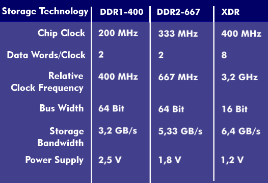
The type designation of the memory chips contains the relative clock frequency that results from the DDR technology. The memory bandwidth of the memory chip is also indicated in the designation. Thus, DDR400 stands for the PC3200 memory block, whereby the specification of 400 means the relative clock frequency and the 3200 the memory bandwidth of 3.2 GB/s.
The memory bandwidth can be doubled again in dual- channel operation. This results in a data transfer rate of 4.3 GB/s for DDR266 in dual-channel mode, and theoretically 6.4 GB/s for DDR400.
The memory chips use Thin Small Outline Package( TSOP) as package technology, and the memory modules are DIMM modules.