ball grid array (chip design) (BGA)
BGA package (Ball Grid Array) stands for a grid-like array of small solder dots. Such a package consists of the bottom board with the BGA array, comparable to a printed circuit, and the plastic housing above it, in which the electronic components are located. The connections on the bottom of the printed circuit consist of spherically shaped solder pads arranged in a square grid, with connection points recessed in the center of the array.
The BGA design is ideal for SMT technology because the round solder points can be soldered directly to the underlying contacts on the PCB during the reflow process. The connection density is very high and the connection paths are very short.
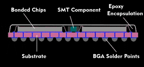
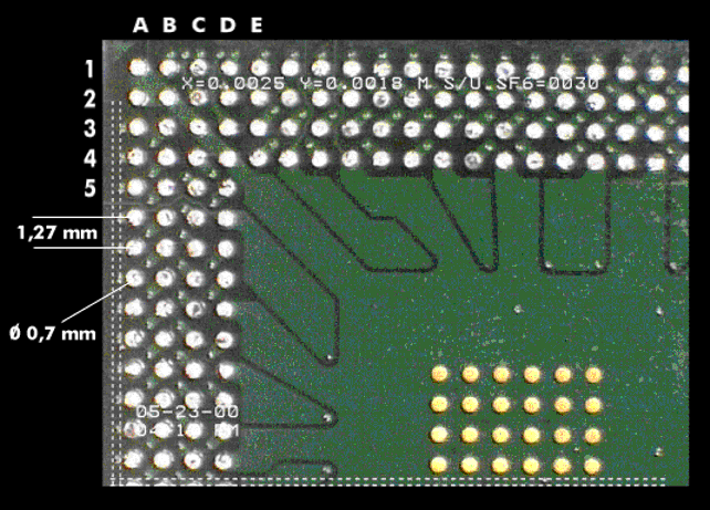
The BGA construction method is also used for BGA packages andsockets. The latter are used, among other things, as CPU sockets for 32- and 64-bit processors with more than 200 connection pins. BGA packages are available with 256, 352, 420 and 560 connection points, which are positioned at a distance of 1 mm or 1.27 mm (1/20 inch). The connectors are marked with numbers in one axis and letters in the other axis. Port "A1" is at the point of marking, which is the corner of the BGA package that has no notch.
During assembly, the BGA package is mounted on a BGA adapter. During this process, the solder pads are heated during reflow until they melt and connect to the contacts on the adapter. Since the distances between the individual connection solder pads are only 1 mm or 1.27 mm apart, precise positioning of the chip is essential. If the distance between the connection solder points is less than 1 mm, this is referred to as µBGA packages.
BGA sockets, which accommodate the BGA adapters, are available for SMT technology and for mounting with a breadboard. They can be temperature resistant or flame retardant and resist infrared heating during assembly. The BGA package is also available in a ceramic version as CBGA (Ceramic BGA). It is smaller and thinner than the plastic PBGA package.