blind via
In the production of multilayer PCBs, there are different techniques to contact the upper or lower solder or assembly side with each other or with an inner PCB layer. These contacts are called vias.
A distinction is made between vias that connect the two outer layers of the board, i.e. plated through holes ( PTH), vias that connect an outer layer to an inner layer, i.e. blind vias, and buried vias.
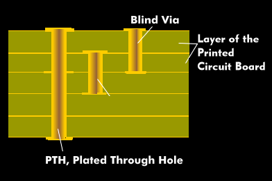
Blind vias are contacts that extend from the assembly side or solder side to an inner PCB layer and are covered by later applied PCB layers. The hole diameter of blind vias is between 0.2 mm and 0.5 mm, the maximum drilling depth depends on the hole diameter and corresponds to the hole diameter. A special form of blind holes are those that connect two internal PCB layers. They are called buried vias and are covered on both sides by PCB layers applied later. A special form of buried via is the semi-buried via. It is a false, capped blind hole.