dual inline package (DIP)
The Dual Inline Package (DIP) describes a package for components. In this design, the pins are arranged in two rows; on both sides of the component package. The DIP design is used for memory devices and other active and passive components: For central processing units( CPU), amplifiers, DIP switches, comparators, resistor networks, LAN controllers, LED units, etc.
The DIP design does not say anything about the number of pins arranged on both sides of the long side. There are DIP devices with 8, 14, 16,18, 20, 22, 24, 28, 32, 36, 40, 42, 48 and 64 pins. As standard, the DIP package comes in package widths of 7.62 mm (0.30"), 15.24 mm (0.60") and 22.86 mm (0.90"). The connector pins are spaced 1/10 inch(2.54 mm) apart, taper down and are angled.
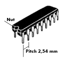
In addition, the package has a groove to prevent incorrect installation. Pin counting is done with pin "1" located to the left of the groove. The last pin is located to the right of the groove.
A disadvantage of the DIP design is that the manufacturing costs are relatively high due to the size of the package. In addition, the inner bonding wires connecting the outer contact pins to the bond pads on the dice are long and have inductive and capacitive influences, which results in a limitation of the characteristics. In addition, the hotspot of a DIP package is relatively large and occupies a large space on the PCB.
Sockets for DIP packages are available in various designs for through-hole technology( THT) and in SMT technology for direct mounting on the PCB surface, and also with locking. The Dual Inline Package is available in ceramic design as CDIP, in plastic design as PDIP and with smaller pitch as SDIP (shrink).