integration density
Integration density is a term used in chip technology. Thanks to a rapid technological development of the integrated circuit, the circuit density on a chip has been increased by many orders of magnitude since the first chips were presented. Specifically, the number of transistors has increased from less than 100 per chip in the 1970s to over one billion (`10^9`) in 2011.
This development could only be achieved by reducing the structure widths in integrated circuits. While this was still 10 µm at the end of the 1960s, it was already 3 µm at the end of the 1970s, 1 µm in the 1980s and only 0.18 µm at the end of the 1990s. Newer technologies work with 300-mm silicon wafers and a structure width of 65 nm, 45 nm, 32 nm, 22 nm and, since 2014, also with 14 nm.
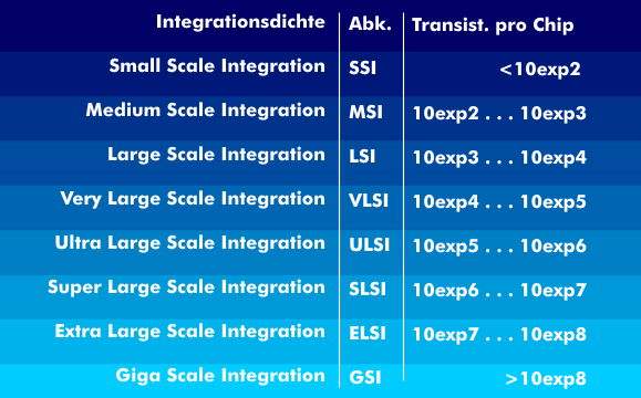
To classify integration technology, the acronym of Scale Integration( SI) has been extended to include terms such as Large (L) and Ultra Large( UL), resulting in the abbreviations SSI for Small Scale Integration, MSI (Medium), LSI (Large), VLSI (Very Large), ULSI (Ultra Large), SLSI (Super Large), ELSI (Extra Large), GSI (Giga), GLSI (Giant Large), and in addition, each technology has been assigned a number of transistor circuits. The boundaries are fluid, but provide sufficient indication of the number of transistors that can be found on a chip.