land grid array (Chip) (LGA)
Land Grid Array (LGA) is a package design. In contrast to Ball Grid Arrays( BGA), this technology does not have spherical contact surfaces, but flat connection contacts.
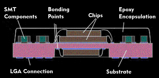
In LGA packages, contact is made via spring-loaded pins in the corresponding sockets, which means that LGA devices are subject to little mechanical stress during installation and removal. In addition, LGA packages are very compact and extremely flat, allowing a high component density. When installed, the height of a CSP package is only 0.68 mm. An LGA package can contain SMD components and bonded chips. The entire device is embedded in epoxy.