pad
Inelectronics and PCB technology, a pad is a contact point or soldering area to which the components are soldered on the PCB.
In plated-through components, the pads are vias that extend through the entire thickness of the PCB. For SMT devices, the pads can be solid copper on the surface or underneath the device, such as in ball-grid array( BGA) and chip-scale packaging( CSP) configurations.
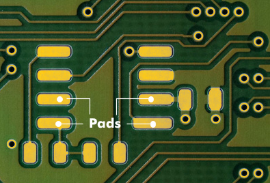
In chip technology, a pad is a solder ball for bonding; also called a bond pad. On printed circuit boards, a pad or solder pad is a solder pad or the solder area for an electronic component. The pad is a widening of a conductor track over which the electronic components are connected to the conductor track.