quad flat no-lead (package) (QFN)
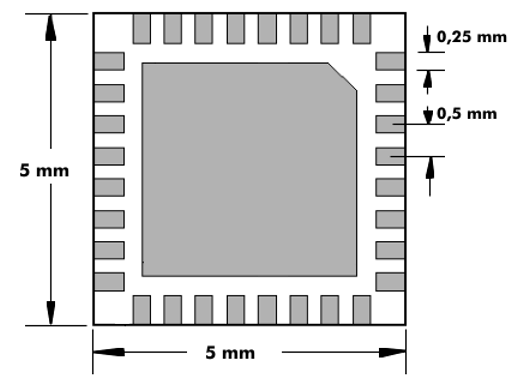
The QFN package (Quad Flat No-Lead) belongs to the various no- lead packages for SMT technology. QFN packages are SMD components that have no connection wires, but connection contacts on the underside of the package with which they are mounted directly on the PCB. The connection pads are on all four sides of the package.
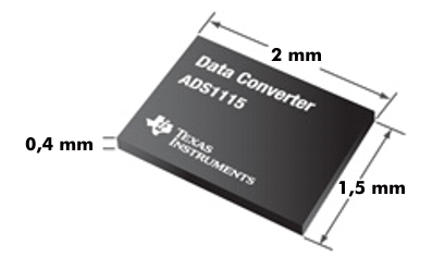
The QFN package is a plastic miniature package that comes in sizes of 1.2 mm x 1.5 mm, 1.6 mm x 1.6 mm, 2 mm x 2 mm, 3 mm x 3 mm and 5 mm x 5 mm. The thicknesses range from 0.4 mm to 0.9 mm.
The footprint is compatible with some packages such as that of the Small Outline Transistor( SOT) and the Thin Shrink Small Outline Package( TSSOP), but it is about 60% smaller than that of TSSOP. The thermal properties as well as the inductive and capacitive connection values have been significantly improved compared to TSSOP.
QFN packages are available with 14, 16, 20, 24 and 32 connections. Because of their compactness, QFN packages are ideal for mobile devices, for cell phones, PDAs and other mobile consumer devices. In addition, QFN is available in flip- chip technology as FC-QFN and as VQFN (Very-Thin) an extremely flat version.
The QFN package was developed by Texas Instruments, Integrated Device Technology by Hitachie.