silicon (Si)
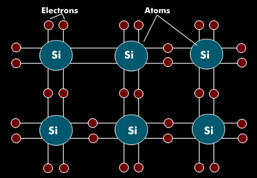
Silicon (Si) is a chemical element with semiconductor properties that is used in highly pure, monocrystalline form in microelectronics. The atoms of silicon are arranged in a regular lattice. In the valence band, the silicon atoms have four electrons that are firmly connected to the electrons of the neighboring atom. Silicon has the atomic number 14 in the periodic table of the elements.
The band gap between the conduction band and the valence band is relatively small and is 1.1 electron volts( eV). If an electron is torn out of the electron bond by the addition of energy, it can be used for charge transport, leaving a hole at its former position. The charge transport can be increased by further freed electrons and by additional added electrons. These additional electrons are inserted by selective impurity, doping.
Silicon is used in electronics in active electronic components and in photovoltaics in solar cells.
The different forms of silicon
Silicon can be manufactured in high-purity form with a monocrystalline structure, but also in polycrystalline and non-crystalline, amorphous structure. Monocrystalline silicon (c-Si) is high-purity silicon in which the atomic structures are arranged in a regular, aligned crystal lattice. Monocrystalline silicon is drawn in a silicon melt to form single-crystal silicon cylinders called ingots, which form the base material for the wafers. For this purpose, the silicon cylinders are sawn into thin silicon wafers, which are used for the production of integrated circuits and solar cells. However, pure silicon only absorbs wavelengths up to 1,100 nm.
Polycrystalline silicon (p-Si), also known as polysilicon, has a multicrystalline structure and consists of many individual crystals. The crystals are about 10 µm in size and have a regular structure within themselves, but they are irregularly arranged in the silicon block. During production, it is cast into silicon blocks that are sawn into thin slices. The molecular structure of polycrystalline silicon is coarser than that of monocrystalline. This semiconductor material can be produced more cheaply and is used in photovoltaics, among other applications.
Sharp has further developed polycrystalline silicon into Continuous Grain Silicon(CG-Si) using Low Temperature Poly Silicon (LTPS). Continuous Grain Silicon is characterized by larger, regular crystal structures with uniform size and expansion. Electron mobility is many times - about 600 times - higher than that in amorphous silicon. This makes it possible to develop displays whose pixels have shorter response times.
Amorphous silicon (a-Si) does not have a regular crystal structure, nor does it have a crystal face. This material, which can be resin or glass, has no solid structure. It has a high absorption capacity, can be produced inexpensively, but has poorer electronic properties than poly- and monocrystalline silicon. In photovoltaics, it is used with optimized microstructure. Other non-crystalline semiconductors include cadmium sulfide, cadmium telluride( CdTe) and copper indium diselenide( CIS). The efficiency of amorphous silicon, at about 8%, is only about half that of polycrystalline silicon. Monocrystalline silicon has the highest efficiency in photovoltaics at 20 % to 22 %.