structure width
The term structure width is used in integrated circuits(IC) and characterizes the technical feasibility of the width of the current paths and the dielectric areas. The structure width is specified in micrometers (µm) or nanometers (nm) and depends largely on the development of photolithographic processes, but above all on the wavelength of the light, since it cannot be narrower than the light wavelengths. These lie in the visible range between 380 nm and 780 nm.
While the structure width of chips in the 1970s was 10 µm for the 4004 with LSI technology and VLSI technology, and 3 µm for the 8086, it was increased to less than 1 µm in the 1980s with ULSI technology. In the 1990s, structure widths of the order of the light-wave length were achieved with SLSI technology.
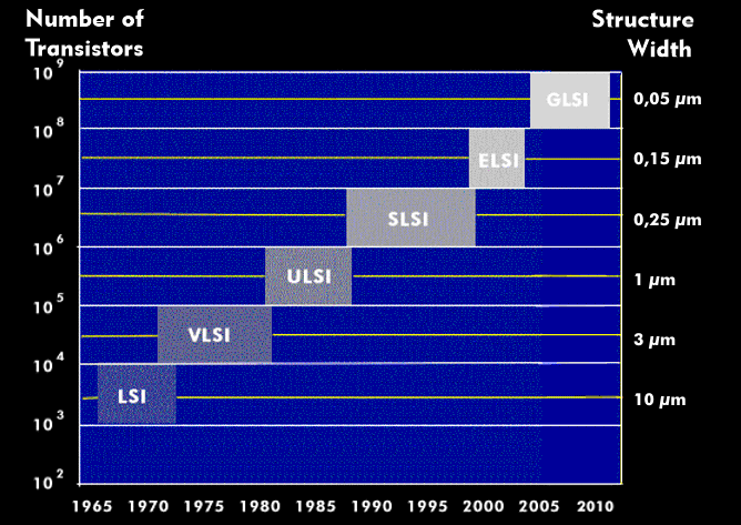
Since photolithographic processes using visible light no longer permitted higher resolution, UV light and then extreme ultraviolet light( EUV) were used for lithographic exposure. The process is therefore called Extreme Ultraviolet Lithography( EUVL). EUVL can be used to realize structure widths of 45 nm, 20 nm and 10 nm. In IBM laboratories, nanochips with structure widths of 2 nm have already been developed.
The structure width directly influences the integration density: The smaller the structure width, the higher the integration density.