transistor package
Transistor housings protect the transistor against mechanical deterioration, as well as against chemical and moisture influences. Such a housing can be made of metal or plastic and have different designs and sizes.
In terms of design, transistor packages can be divided into two main groups: Diode Outline( DO) for diodes and Transistor Outline( TO) for transistors. These two types are available in small outline versions as small outline diode (SOD), small outline transistor( SOT) and for small outline integrated circuits( SOIC) as small outline ( SO). They are distinguished by their production-related use on printed circuit boards. The TO design is for through-hole technology, while the SOT designs were developed for SMT technology.
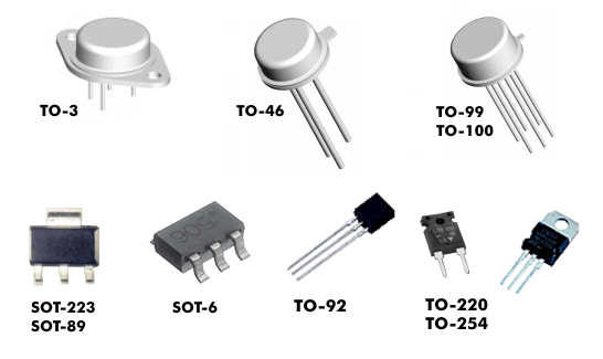
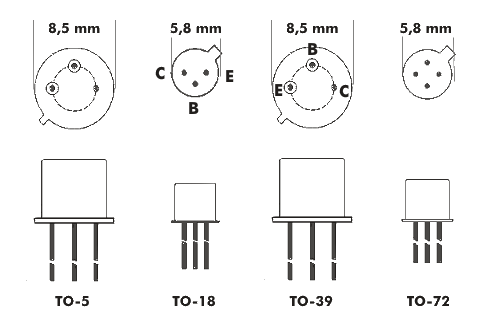
Transistor packages in TO design can have a round housing; however, they are also available in a flat housing (TO-220 and TO-254) for direct mounting on the chassis or PCB; the TO package can furthermore be made of metal or plastic. The individual variants depend on the application and the transistor power. For example, the TO package includes small- signal transistors (TO-18), transistors for low power up to 1 W (TO-5 and TO-39), for medium power (TO-66), and high power (TO-3 and TO-254).
In addition to the transistor power, the size of the TO package depends on the number of leads. Since there can be two transistors or one transistor circuit in one transistor package, there are round packages with 6 pins (TO-78) or with 10 pins (TO-100).
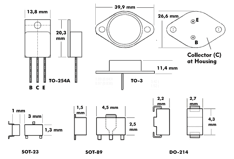
The SOT package meets the increasing requirements for smallest dimensions. Components in SOT packages have dimensions in the low single- digit millimeter range. For example, the SOT-23 has dimensions of 1.3 mm and 3.0 mm, with a thickness of 1.0 mm. Smallest SOT packages are only 0.8 mm wide and 1.6 mm long.