vertical interconnect access (PCB) (via)
The abbreviation Via stands for Vertical Interconnect Access, a vertical electrically conductive connection. Vias are plated-through holes on a printed circuit board; they are also referred to as layer changers or vias. Such vias are used exclusively for through-plating between several layers of a printed circuit board, via which an electrically conductive connection is established. They are not suitable for components processed using through-hole technology( THT).
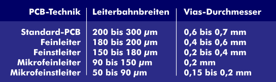
Vias have a small hole diameter and connect different layers of PCB with each other. The hole diameter depends on the trace structure and is 0.60 mm for standard traces, reduced to 0.40 mm for traces in fine condu ctors and down to 0.20 mm for ultra-fine conductors. The even smaller microvias are 0.20 mm and 0.15 mm.
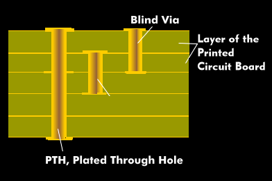
If the vias contact the two outer layers of the PCB with each other, these are through vias, plated through holes or plated through holes( PTH). If the traces of two inner layers are connected to each other, these are called buried vias. These vias enable complex layout structures and high circuit density. They are only possible with multilayer PCBs and are not accessible from the board surface.
If the vias connect the top or bottom copper-clad layer to an inner layer, they are blind vias or blind holes. Blind vias start in the PCB surface and extend to the desired inner PCB slot. And plugged vias are sealed vias. Plugged vias can be placed under the spherical solder pads, the balls or bumps, of BGA packages and their variants, which simplifies PCB unbundling.
With small trace distances, the vias become increasingly smaller, which is then referred to as microvias. There is also a through- silicon vias( TSV) technology, which is used in semiconductor technology, optoelectronic components and microsystem technology( MST).
The holes for the vias can be drilled with microdrills, burned by lasers or punched as in Low Temperature Cofired Ceramics( LTCC).