circuit board production (PCB)
PCB production is a complex multi-stage process in which an electronic circuit diagram is converted into a functional board populated with components. The basis for PCB production is the electronic circuit diagram, the copper-clad base material and the parts list with the characteristic values of the components, their power consumption and their dimensions. Printed circuit boards are designed with CAD systems and manufactured with CAM systems.
Placement of components
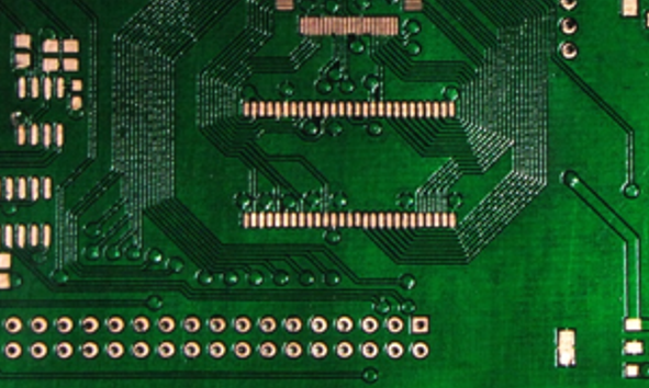
In the first stage of PCB production, after determining the size of the PCB, the components specified in the schematic and the bill of materials, which are stored in a database, are placed on the PCB in such a way that they have the shortest possible connections. Component placement is done with CAD programs, taking into account the component dimensions stored in the database.
The printed circuit board unbundling
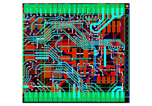
Prior to PCB routing, the placed components are connected to each other according to the circuit diagram, using the shortest possible route. Depending on the complexity of the circuit, more or less lines cross. These must be routed without crossing, which is the task of the track un bundling process. During PCB routing, certain design rules must be observed for placement optimization. These can be that the components are aligned in as one direction as possible, or that signal-carrying lines are as short and direct as possible and are routed with a minimum distance to other signal-carrying lines. In addition, the power supply and ground should have their own PCB plane. Unbundling also determines the number of layers on the board, as well as vias and other vias.
Design rule compliance isverified with a design rule check, or DRC. This determines whether all design rules are adhered to and no logical errors are contained. These can be short circuits between crossing traces or missing contacts of components.
The files calculated during routing are Gerber files, which are used for board exposure, soldermask, drillings, fiducials, etc.
Etching the PCB
Before the PCB is etched, the resist for the soldermask is applied. After exposure, this photoresist is removed from the areas where no copper is to remain. In the following etching process, the individual layers are produced. For this purpose, the calculated traces, ground planes, vias, solder pads, etc. are etched out of the copper-clad and exposed PCBs. This can be done chemically or electrolytically. The layers are then pressed together to form a printed circuit board with an accurate fit.
The assembly of the printed circuit board
Before the printed circuit boards are assembled, the solder resist masks (resist) made of peelable lacquer are printed on, and vias and holes for component wires or pins of chips are sealed so that they do not become clogged with solder during the soldering process. This is followed by placement, which is carried out manually for small quantities and automatically with an automatic placement machine for larger quantities. The components to be assembled are taped in the correct sequence or pre-sorted in plastic trays before the placement machine positions them correctly.
Soldering the components
After component placement, the components are soldered onto the printed circuit boards. The soldering process used depends on whether the components are mounted using through hole technology( THT) or SMT technology. Wave soldering and dip soldering, which can be used for single-sided boards, are suitable for through-hole technology, while reflow is used for surface-mounted technology (SMT).
After the assembled boards have been cleaned, they are subjected to a wide variety of optical and electrical test procedures.